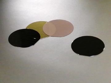
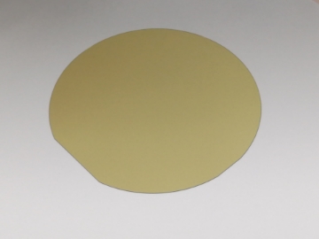
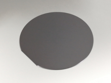
RF Bonded Wafer
RF Bonded Wafer
Bonded Wafer Typical 3 Layer Structure for TC-SAW & TF-SAW Piezo Layer is LT-120YX or Any Other Cut Angle.
 Contact sales for preliminary SPEC
 -
Polishing
- Surface Roughness Sa<0.2nm, Sz<2nm
- Piezoelectric layer Thickness > 400nm (Tolerance ±20nm)
-
Cleaning
-
Particle < 0.5μm
Intermediate film sputter formation
Various Film sputter formation (RAS & etc)
Room temperature wafer Bonded
Bonded as atomic level (nano scale)
-
Particle < 0.5μm
-
Positioning Accuracy
-
X-Y alignment <0.3mm
θ alignment <0.3
-
X-Y alignment <0.3mm
-
Bonded Strength
- eg : LT/Si >1J/m2/Ave 1.9J/m2
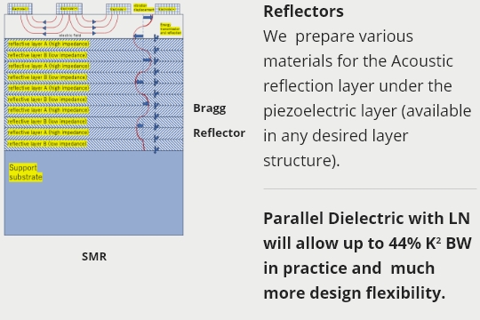
Multi layer Structure Bonded Wafers for SMR type filter (Piezo Layer is rotated Y cut LT or LN (Vertical or Parallel Dielectric)
Our bonded wafers can be structured with various cut angles and various piezoelectric crystals. Our wafer technology can be used for 5G Wide Band communications allowing for design flexibility needed by designers. Our design staff is well versed in crystal and piezo design structures.
BAW SMR Filter published at Acoustical Society of Japan (ASJ) Sept 2021 by our designer Eguchi.
Product Road Map
Siward plans to extend portfolio to filter using in house processed piezo multi wafer as a goal, and focus to the design with high RF and wide BW required for 5G Sub-6GHz band first, and extend to mm wave, and NB-IoT, aerospace, and other high RF application.
Wafer
Main Application
- for SAW/BAW/Lamb wave Device.
- Piezoelectric (/silicon) multi function Layer.
- Various material combination is possible.
- Fine performance of thickness control (Tolerance +/-20nm/ eg ) including fine flatness (warp, Bow, TTV and etc).
- Any Crystal orientation is selectable.
- Development to achieve high electromechanical coupling coefficient (K2) and temperature coefficient of Frequency (TCF) by piezoelectric materials.
Filter
Main Application
- WLP products for RF BAW/SAW filters. (Design for BAW filter is ready initially)
- Strength for 5G Sub-6GHz and Wi-Fi RF top filter, and undertake more higher frequency depend on requirement.
- Optimal substrate selection per multilayer for high K2, acoustic velocity, and fine TCF to achieve high frequency, wide BW, and other electrical parameters.
- Experienced for Ladder and Lattice circuit configuration to achieve optimal pass band and out of rejection.
- Sputter etching technology and facility enabling multi reflection (bragg) layer to improve high Q and heat dissipation performance.
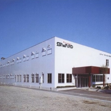
Siward Japan
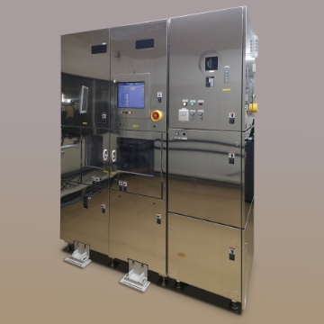
Focus on wafer for RF device, and RD/Manufacturing site in Yonezawa, Japan
01
Engineering and manufacturing piezoelectric bonded multi layer wafer.
02
Main application is for RF BAW/SAW filter selected by 5G (Sub-6GHz), NB-IoT, WiFi and other high RF wireless equipment.
03
Structured design flexibility with various cut angle/piezoelectric crystal with thin film by Siward well versed engineering staff in crystal and piezoelectric design structure.
04
Develop to achieve electromechanical coupling coefficient (K2) as Wide BW.
Contact
Siward TECHNOLOGY CO., LTD.
- ADD : 1-1-37 Tohrimachi Yonezawa-city Yamagata-pref 992-0025 Japan
- TEL : +81-238-23-3305
- FAX : +81-238-23-3308
- staff1@siward.co.jp
- https://www.siward.co.jp